When it comes to PCB Design, not all design parameters are as stringent or clearly laid out as military specifications, or mil-spec. There aren't always clear guidelines for a given project, even if the design intent is clear. Because of that, you instead must fall back on industry best practices for PCB design.
You should always attempt to follow best practices in any project, regardless of special instructions. Not sure what the industry best practices are for PBC layouts or PCB design basics? Don't worry, we're here with the guidance you're looking for.
 Fundamentals of PCB Design
Every industry has its own essential steps or concepts you can't live without. Apart from standards, which change with technology, there are also quality of life and safety concerns. Following industry best practice comes down to fundamental design ideology and workflows. In PCB design, those practices are a list of principles which include:
- Use correct grid spacing
- Avoid multiple grids whenever possible
- Keep your traces short and direct
- Be cognizant of your power distribution
- Component groupings simplify designs and testing
- Perform a design rule check (DRC) as often as you can
- Use silkscreens to their full potential
- Try to stay away from auto-routers
This is by no means a full list of considerations for PCB design. Rather, these are fundamental principles and steps that you cannot skip or put off. Let's dive into a few of these now.
Grids and Spacing
A PCB running on multiple grids is more prone to being a failed design. This is due to increased complexity and possible polygon-fill issues. It may seem appealing and interesting to work on multiple grids or polygon shapes. Using the same polygon and grid throughout your PCB will ensure that you avoid spacing issues.
Just as important as shape, making sure to adhere to spacing requirements avoids shorts. It also keeps electromagnetic interference (EMI) issues down. Following spacing guidelines on keeping trace lengths as short and direct as possible helps with a variety of serious problems. A few of these are:
- Security
- EMI
- Heat dissipation
- turning your PCB into an antenna
- Ground faults
Keeping your components group related on your grid will help you to avoid these problems as well. Keeping traces direct and short will reduce 90° bends in traces, which can easily become shorts. Sticking to direct and short routes will help to increase more gentle 45° turns in traces. Along with smaller and more direct traces, keeping loops small reduces inductance and HF voltage spikes.

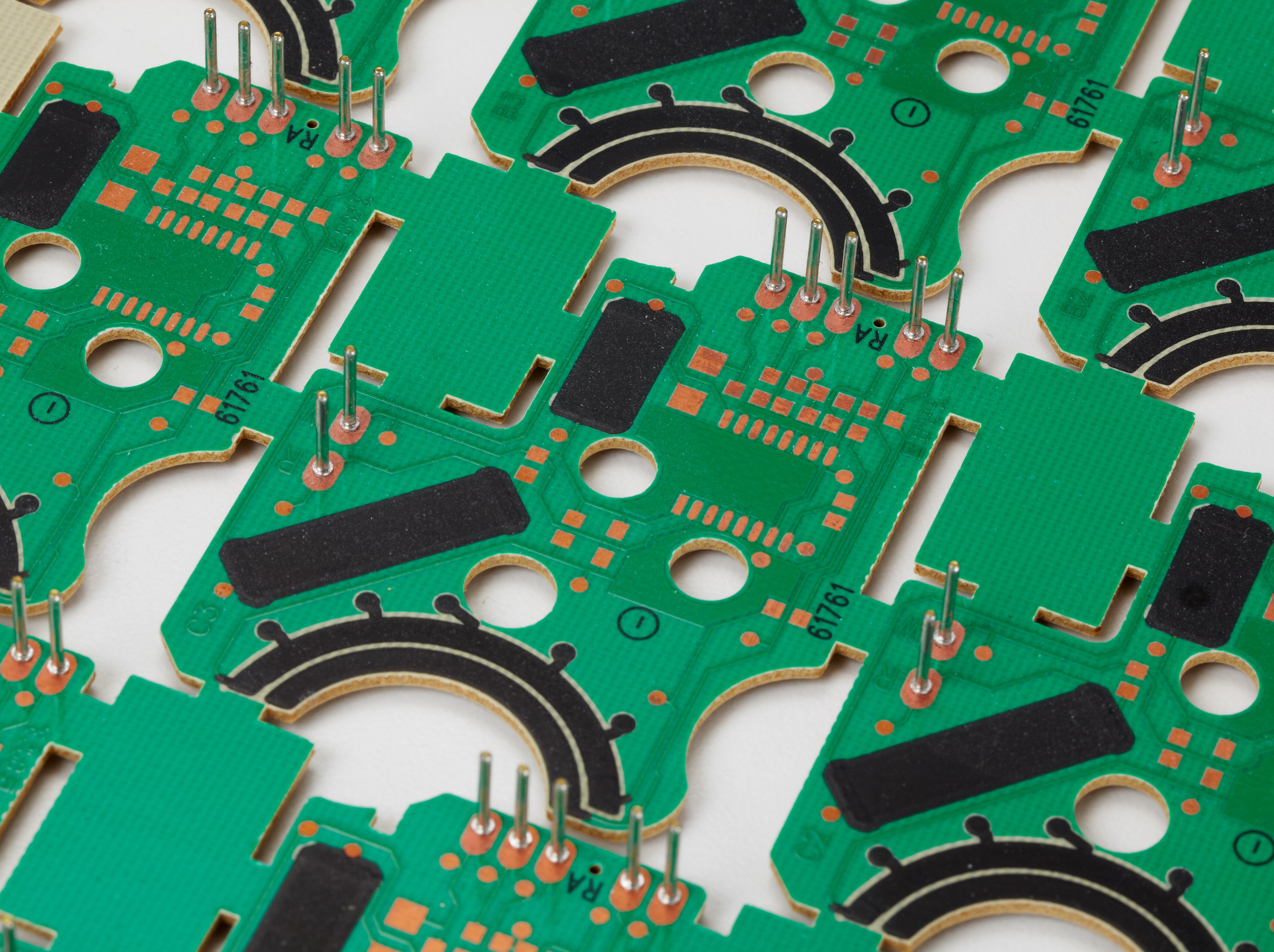
Clearly Label With Silkscreen
 One of the most important points of PCB design has nothing to do directly with the function. As we design traces, component location, grids, and grouping to direct the flow of electrons, we also must consider silkscreening. Silkscreening makes the process of manufacture, user function, testing, servicing, and engineering much easier.
Silkscreening effectively is a quality-of-life decision. You can make life better for yourself and everyone else who touches the board with adequate silkscreening methodology. Even if silkscreen annotations are hidden under components, they've done their job well. Surprisingly, as you go through the process of labeling on your silkscreen layer, you may find design flaws you hadn't previously considered. Making sure to use silkscreen on both sides of the PCB helps to streamline production.
Power Planes and Ground Planes
Power planes are flat planes of copper connected to the power supply. The ground plane is connected to a ground connection for the power supply as well. Both of these planes are essential to effectively power and ground your PCB design.
That being said, only PCBs with four or more layers will have power planes in them. Power planes have three giant returns on your design investment. They give shorter paths, improve circuit decoupling, and increase current carrying capacity. Traces can only hold so much current and heat. Their smaller size means that heat will build up in a smaller area and therefore more resistance.
Lower temperature due to power plane utilization means less wasted electricity and better function. The use of vias from the signal layer to the power plane is convenient. use of power plants also creates a decoupling capacitor between itself and the insulating layer. This helps reduce unwanted noise from propagating through the PCB design.

PCB Design Software
PCB design software is also important. Often you can find free software versions if you're just starting out. But to be professional, you'll have to use industry-standard software. The top PCB Design software in use by professionals today includes offerings like:
- Altium Designer
- Solidworks PCB
- Autodesk Eagle
These are not the only ones you must use, but they're common in the PCB design field. Autodesk Eagle also has free licensing for personal use. Whatever you use, make sure it has the capability of generating all the PCB layout files you'll need. Most significantly, a Gerber file or ODB++. Other files you'll need are:
- Centroid or "Pick and Place"
- Bill of Materials (BOM)
- Special requirements (ReadMe text or PDF)
- Assembly Drawings (PDF filetype)
These files are almost always the minimum requirement. There may be more, depending on the product and client specifications.
PCB Design Essentials and Best Practices
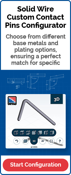
Bead Electronics has experience working with PCB Design and Electrical Engineers. We work with you and your team on optimizing your packaging, pin insertion, and more. We're industry leaders in custom pins and pin assemblies for aerospace and military, healthcare, automotive, and communications devices. Bead Electronics prides itself on its accountability, collaboration, resilience, and ability to evolve with the industry. Contact us today to see how we put these values forward in your project.
About Bead Electronics
Bead Electronics, is a global manufacturer of electronic connector pins and has been manufacturing in Connecticut for over 100 years. The award-winning company carries over 500 patents and is best known for inventing its manufacturing process called swaging. This process is a high-speed, virtually scrap-less, cold-forming process capable of producing a wide size range of metal electronic components that are consistent and cost-effective. The family-owned business is led by its fifth generation. Click here to speak to a connector pin specialist today.