The field of printed circuit board (PCB) design is massive, and growing at a nearly 14% rate today. These circuit boards power so many of the electrical components that we all use and rely on each and every day.
The more you understand about the design of these circuit boards, the easier time you'll have producing the outcomes that you're looking for. These points will help you out when you're looking into the best PCB layout tips and options available.

Understand the PCB Design Steps
Before you look into things like complex semiconductor production or even standard PCB cleanup options, you need to understand the fundamentals of the PCB design process. Having a grasp of these fundamentals will let you know which steps to take, and will let you overcome some common obstacles that come with the territory.
Begin with an understanding of your goals for the circuit board, in addition to the basic electrical power specifications that you're going to be working with. This means understanding things like:
- The location of connectors and circuits
- The maximum allowable current and voltage
- Different types of signals that you're dealing with
- Considerations for shielding
- The PCB impedance characteristics
From here, you'll know what kind of power you're dealing with and can plan accordingly.
Next, make the schematic, and design the optimal PCB layout. You will be able to then create a stackup, figure out requirements, and set your components into place.
This is a careful and strategic undertaking that will require your full attention and some skills and knowledge.
Take Your Time When Going to the Autorouter
So, what's the first thing you should know about handling your PCB layout cleanup? For one, don't be in such a rush to take the project to the autorouter. It's a feature in the PCB design software that lets you figure out several potential routing placements.
This is an incredibly helpful tool, but relying on it too heavily in the beginning can create some potential problems. Relying on the autorouter too much can lead to work that is inaccurate and not to your liking. There's no substitute for human experience, so trust your knowledge and instincts first, and use the autorouter to check your work at the end of the process.
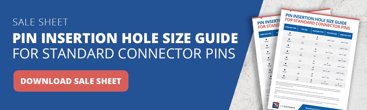
Double-Check Your Hole Sizes
Next, make sure that you're double and triple-checking your PCB hole sizes. Generally, hole sizes are driven by the sizes of the devices going into a PCB, such as a connector pin from Bead Electronics. Some people set the size of their holes as they go, only to find that they paint themselves into a corner at some point.
Circuit board cleanup requires you to check these different hole sizes to make sure that they're consistent, and that they fit whatever type of tooling that you're using. It's best to use standard-sized drills so that it's not difficult to match your hole sizes in a way that creates uniformity throughout the entire project.
Adjust Your Vias and Routing
The next part of cleaning up your circuit board layout involves adjusting your vias and routing. Make sure to handle your routing so that you don't deal with clearance errors. Again connector pins and their features (e.g. thru-hole stars, knurls, etc) must be considered for hole sizes and tooling.
When you inspect your vias, you should be aware of any drill size requirements and pad sizes (e.g. surface mount [SMT]). You might also find that you need to apply teardrops as necessary.
Run Through Several Mechanical Checks
Optimizing your circuit board design might also require you to run through several mechanical checks. The best way to do this is by making note of any mechanical requirements in the beginning so that you can inspect them during the process and at the end of it.
Make sure that your connectors fit the positioning of your PCB layout and serve their intended purpose. Once you know that your PCB layout is mechanically sound, lock your elements into place.

Pay Attention to Polygons
Polygons also play a significant role when you're trying to clean up your PCB layout. For one, make sure that you redraw them whenever necessary. Taking this effort will help fix overlapping problems and to avoid the opening of any net connections.
Make sure that copper is evenly distributed across the polygons and layers, and verify that all of your polygons have net assignments.
Conduct a Design Rule Checking (DRC Check)
Before you finish up your work, you will likely need to run a DRC check or two. If you have DRCs that are outstanding, you leave the project at risk.
Make certain that you don't have any rules violations before moving forward to create outputs. Once you take the time to check for these violations, you will have full confidence moving forward with finalizing your design. And then from there, you're just a step away from sending your boards out for final printing.
Optimize Your PCB Layout
The points above will assist you when you're trying to get the most from your PCB layout. This is a potentially complex area of tech that you'll need to address with the best skill and experience. Other tips include adjusting the layout of your layers, setting up a ground plane, and paying attention to your silkscreen layers.
Once you have shored up these types of details, you're in the best position to get the outcomes that you want from your circuit boards.
Bead Electronics looks forward to hearing from you when you're looking for assistance with PCB design for connectors. Take the time to contact Bead the next time you need help with your pins or any other aspect of your electronics manufacturing process.