Have you opened up an electronic device and found all this network of small components? Ever wondered how they work? You find these minute components on the circuit boards of your cellphone, laptop, and microwave, etc.
Rather than using common components, printed circuit board manufacturers install these components onto the surfaces of the boards using advanced devices. It is important to remember that the bulk of them are relatively small in size. Surface Mount Technology (SMT) is the name given to the technology used to mount these devices. So, what exactly is SMT and what are its benefits?
SMT board components and connectors come in three separate models to accommodate a wide variety of device designs. Here is everything to know about through-hole wave soldering, press-fits, and SMT.

What is Wave Soldering?
Wave soldering is a wide-scale soldering procedure that involves soldering electronic components to a printed circuit board (PCB) to create an electronic panel. The name comes from the fact that the method uses a tank to store melted solder.
You add the elements to the printed circuit board (PCB). The PCB is then dipped into a pumping wave or cascade of solder. The solder adheres to the uncovered metallic areas of the board. That establishes a close mechanical and electrical attachment.
The method is much simpler and can produce a better quality result than manual soldering. You use wave soldering for both through-hole and surface-mount printed circuit assemblies.

What is SMT?
Surface Mount Technology is the method of connecting electronic components to the top and/or bottom surfaces of printed circuit boards (PCBs). Surface Mount Technology varies from wave soldering and is the ideal substitute or solution to press-fit or wave solder technologies. Because of the high levels of automation and precision provided by SMT technology, smaller assemblies with repeatability can be achieved.
Many manufacturers are now using this technology because it helps them to easily build small PCBs that are lightweight and compact. SMT is a straightforward method that involves simply placing and positioning PCB components on a board.
If you are considering using SMT technology in your PCB assembly, you will undoubtedly reap some of its advantages:
- Cheaper Manufacturing: SMT allows for the production of smaller PCB designs, resulting in lower production costs. SMT allows components to be placed next to each other on the board.
- Improved Efficiency: Another explanation why many PCB manufacturers seem to like SMT is work efficiency. Using SMT, assemblies can be completed in one single day and in the shortest amount of time unlike press-fit technology, which may take some time.
- The SMT Structure is Less Complicated: The general configuration of the boards you get to produce with SMT is straightforward. SMT mounted boards do not necessitate a lot of technicalities. Panels made with SMT have more simplistic configurations than those made with other methods.
- And Less Vulnerable to Errors: Another advantage of SMT technology is that it's possible to correct small mistakes quickly and easily. SMT, in comparison to comprehensive wave solder, is not as careful with detail, making it possible to correct small mistakes for boards. Manufacturers favor this approach because it allows them to manufacture a large number of boards with fewer mistakes.
- Superior Efficiency of Electromagnetic Compatibility (EMC): With SMT, it is possible to obtain a lightweight bundle together with lower lead activation. You can be assured of a limited radiation circuit field, which means excellent EMC efficiency.

What is a Press-Fit?
Many of today's new electronics make use of solderless, press-fit part technologies to add versatility to their products. You make high-quality, electrical links possible by press-fit technology.
A press-fit connector's parts are placed into through-holes in the printed circuit board, where friction is exerted due to the deformation of the press-fit bits. The snug fit keeps the contact pins close allowing electricity to flow through.
A press-fit connector's pins are inserted into through-holes in the printed circuit board. It is where friction is exerted due to the deformation of the connector's press-fit legs. The snug fit keeps the contact allowing electricity to flow through. Press-fit pins provide a dependable connection that naturally disperses a higher thermal heat and has a lower failure rate than with solder joints.
Another advantage of press-fit is thermal compatibility. If you need to do a second solder on a PCB, the heat from the solder can damage the PCB and linked electronic components. Press-fit technology, on the other hand, eliminates the use of heat and allows new press-fit components to be added without damage.
Some of the main reasons behind the increased use of press-fit include:
- Removes the likelihood of dry joints, breaking, and other soldering concerns
- Interfaces that are strong, solder-free, reproducible, and highly reliable
- Methods for testable assembly with combined force control
- Press-Fit integration processes that are streamlined for predictable performance
- Interfaces for direct contact
- Outstanding electrical and thermal transfer properties
- Power applications need a high current carrying capacity.
Because of these major advantages, press-fit technology has become a popular solution for the production of many new goods. It has also resulted in a spike in the number of design improvements to products switching from solder-based connectors to press-fit manufacturing. All in all, press-fit connectors are less expensive, easier to rework, and more environmentally friendly.
Wave Solder vs. SMT vs. Press-Fit
While there has been a shift away from wave solder in some implementations over the last two decades, there are still many legitimate applications for this process. That is because of its reliability. However, based on product accessibility and volume, SMT and press-fit both have their own applications that are now very well-established. Your decision about which technology to use, wave solder vs. press-fit vs. SMT, must be made early in the concept design phase, as it will affect the choice of connectors and other equipment. Make sure you have all of the necessary knowledge and do some product research.
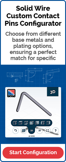
Need more information on our custom contact pins? Contact us and send us your design!
About Bead Electronics
Bead Electronics, is a global manufacturer of electronic connector pins and has been manufacturing in Connecticut for over 100 years. The award-winning company carries over 500 patents and is best known for inventing its manufacturing process called swaging. This process is a high-speed, virtually scrap-less, cold-forming process capable of producing a wide size range of metal electronic components that are consistent and cost-effective. The family-owned business is led by its fifth generation. Click here to speak to a connector pin specialist today.